by Tiwari Academy Team
NCERT Solutions for Class 12 Physics Chapter 14 Semiconductor Electronics Materials, Devises and Simple Circuits in Hindi and English Medium for session 2026-27. The chapter 14 is alter for exams as a particular portion of the chapter is deleted. Get here the modified and revised solutions of chapter 14 of 12th Physics based on NCERT books for 2026-27 exams.
Viva Questions for Class 12 Physics Practical
How to Prepare Class 12 Physics Board Exam
Study Plan Class 12 CBSE Board 2025
NCERT Solutions for Class 12 Physics Chapter 14
Chapter 14 Semiconductor Electronics Solutions
- Class 12 Physics Chapter 14 Exercises Solutions
- 12th Physics Chapter 14 Additional Exercises (Not in Syllabus)
- Class 12 Physics Chapter 14 Solutions in Hindi
- Class 12 Physics NCERT Book Chapter 14
- Class 12 Physics Revision Book Chapter 14
- Revision Book Answers
- Class 12 Physics Chapter 14 Revision Notes 1
- Class 12 Physics Chapter 14 Revision Notes 2
- Visit to 12th Physics Main Page
Get the Exercises & Additional Exercises Solutions in PDF to use it offline as well as view online. UP Board Students can download UP Board Solutions for Class 12 Physics Chapter 14. Download CBSE Offline Apps and NCERT Sols of other subjects also for new academic session 2026-27.
| Class: 12 | Physics |
| Chapter 14: | Semiconductor Electronics: Materials, Devises and Simple Circuits |
| Content: | Exercises and Extra Questions |
| Content Format: | PDF, Images, Text and Videos |
| Academic Session: | Year 2026-27 |
| Medium: | English and Hindi Medium |
Class 12 Physics Chapter 14 Solutions in English
NCERT Solutions for Class 12 Physics Chapter 14 Semiconductor Electronics are given below to download free in PDF form for based on CBSE Syllabus 2026-27. Download Offline Apps and NCERT Books in PDF form for new session. Join the discussion forum to ask your queries related to NIOS and CBSE Board Examination.
Important Questions for practice
1. What is the function of base region of a transistor? Why is this region made thin and lightly doped? Draw a circuit diagram to study the input and output characteristics of n-p-n transistor in a common emitter configuration. Show these characteristics graphically.
2. In an n-p-n transistor circuit, the collector current is 10mA. If 90% of the electrons emitted reach the collector, find the base current and emitter current.
3. A p-n junction is fabricated from a semiconductor with a band gap of 2.8 eV. Can it detect a wavelength of 600 nm? Justify your answer.
4. A carrier wave of peak voltage 12v is used to transmit a message signal. What should be the peak voltage of the modulating signal in order to have a modulation index of 75%?
5. If the current gain of a CE – Amplifier is 98 and collector current Ic = 4 mA, determine the base current.
Questions from Board Papers
1. Semiconductors do not support strong current i.e., a semiconductor is damaged when strong current passes through it. Why?
2. Name the semiconductor device that can be used to regulate an unregulated dc power supply.
3. A semiconductor device is connected in a series circuit with a battery and a resistance. A current is found to pass through the circuit. When polarity of the battery is reversed, the current drops to almost zero. Name the semiconductor device.
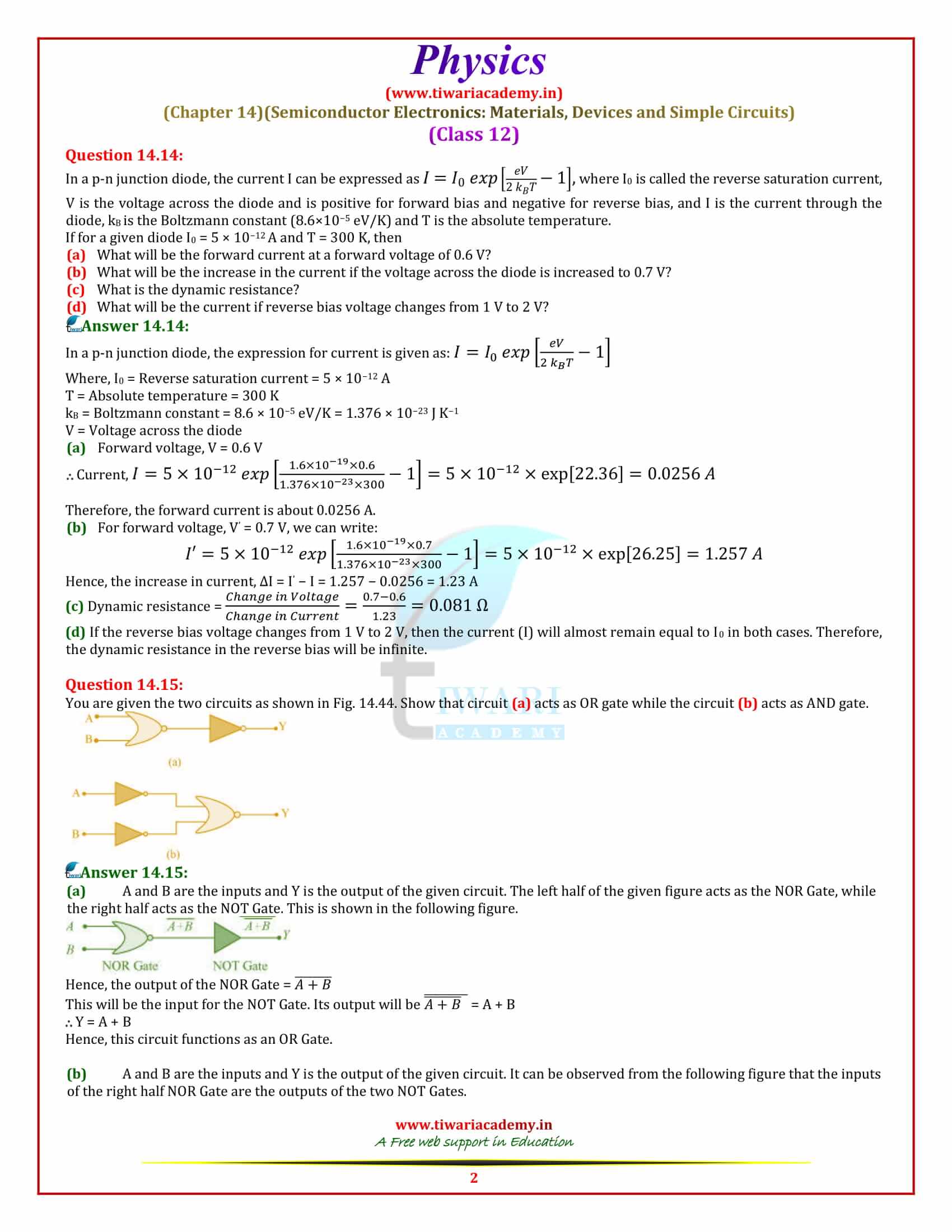
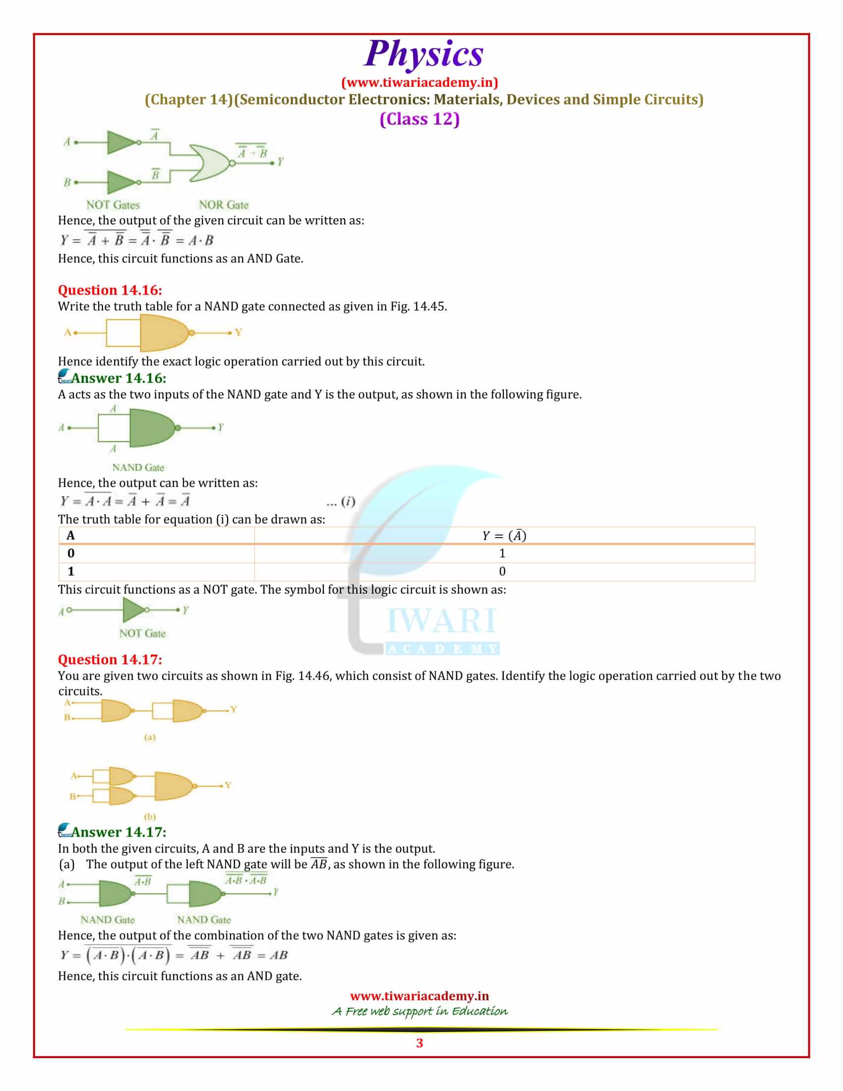
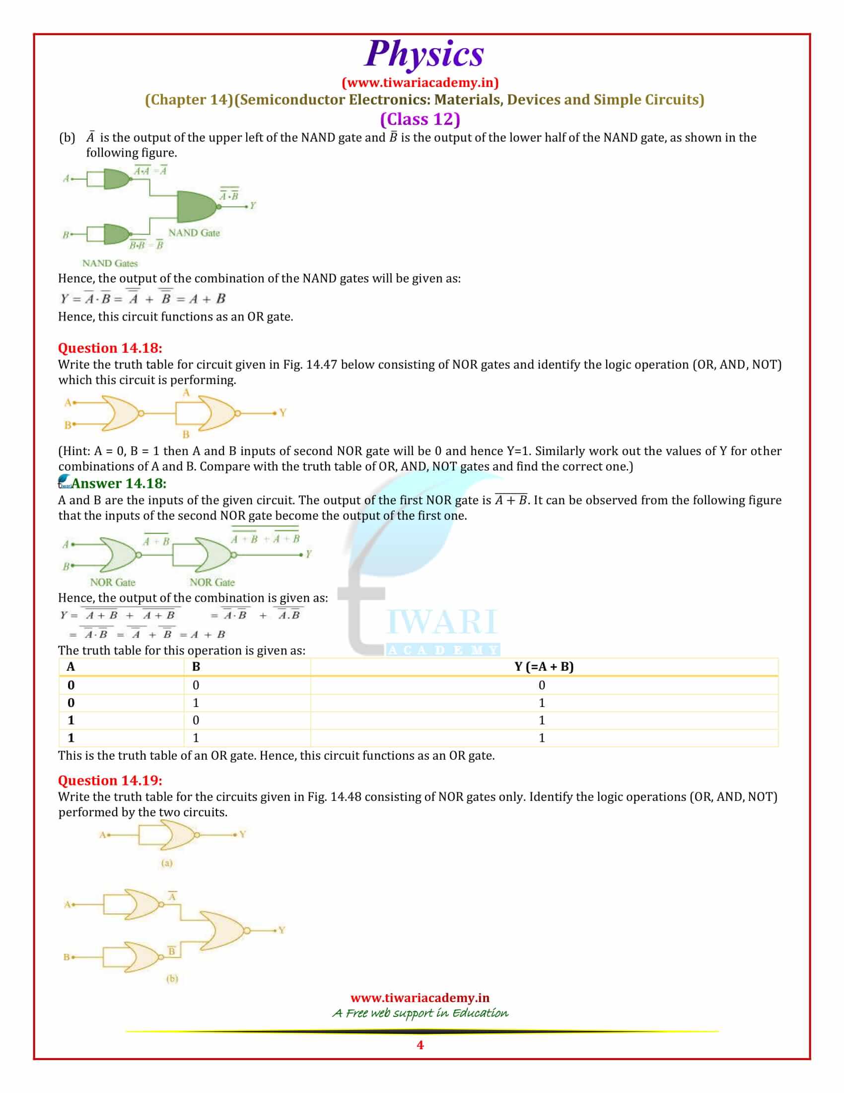
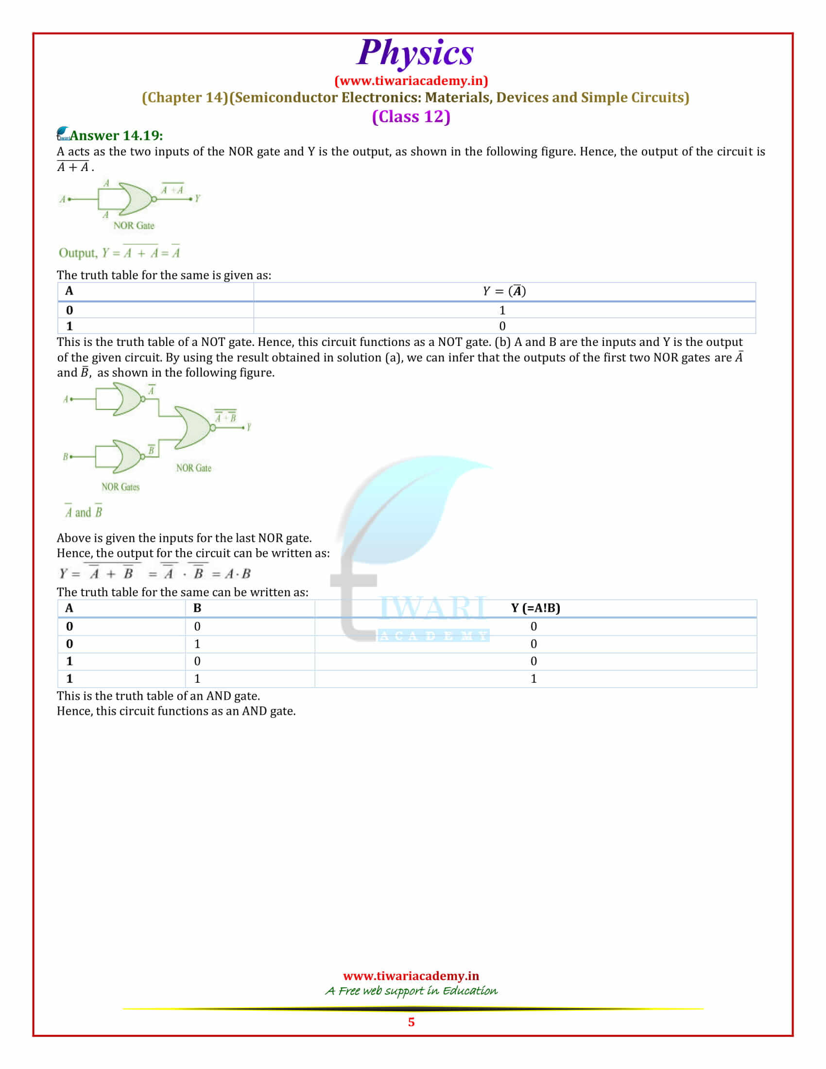
4. The output of a 2 input AND gate is fed as input to a NOT gate. Write the truth table for the final output of the combination. Name this new logic gate formed.
5. Which special type of diode can act as a voltage regulator? Give the symbol of this diode and draw the general shape of its V-I characteristics.
Important Questions on 12th Physics Chapter 14
In half-wave rectification, what is the output frequency if the input frequency is 50 Hz. What is the output frequency of a full-wave rectifier for the same input frequency?
Input frequency = 50 Hz For a half-wave rectifier, the output frequency is equal to the input frequency. Output frequency = 50 Hz For a full-wave rectifier, the output frequency is twice the input frequency. Output frequency = 2 × 50 = 100 Hz
Two amplifiers are connected one after the other in series (cascaded). The first amplifier has a voltage gain of 10 and the second has a voltage gain of 20. If the input signal is 0.01 volt, calculate the output ac signal.
Voltage gain of the first amplifier, V₁ = 10 Voltage gain of the second amplifier, V₂ = 20 Input signal voltage, Vᵢ = 0.01 V Output AC signal voltage = V₀ The total voltage gain of a two-stage cascaded amplifier is given by the product of voltage gains of both the stages, i.e., V = V₁ × V₂ = 10 × 20 = 200 We have the relation: V₀ = V × Vᵢ = 200 × 0.01 = 2 V Therefore, the output AC signal of the given amplifier is 2 V.
Why are elemental dopants for Silicon or Germanium usually chosen from group XIII or group XV?
The size of dopant atoms should be such as not to distort the pure semiconductor lattice structure and yet easily contribute a charge carrier on forming co-valent bonds with Si or Ge.
Sn, C, and Si, Ge are all group XIV elements. Yet, Sn is a conductor, C is an insulator while Si and Ge are semiconductors. Why?
The energy gap for Sn is 0 eV, for C is 5.4 eV, for Si is 1.1 eV and for Ge is 0.7eV, related to their atomic size.
In a CE transistor amplifier there is a current and voltage gain associated with the circuit. In other words there is a power gain. Considering power a measure of energy, does the circuit voilate conservation of energy?
No, the extra power required for amplified output is obtained from the DC source.